
Digital Input
xiQ cameras with older hardware revisions are compatible only with 24V input signals.However, xiQ cameras with newer hardware revisions support 5V digital input (TTL), while staying backward compatible with 24V input signals.
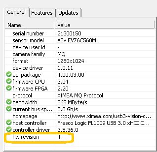
The hardware revision of the camera can be verified using xiCOP according to the following steps:
- Download and start xiCOP
- Select the camera in the XIMEA camera list
- The number of the hardware revision can be seen on the General tab on the right side of the window.
5V-24V GPI
Supported cameras
| Camera model | HW Revision |
| MQ003xG-CM | ≥4 |
| MQ013xG-E2 | ≥6 |
| MQ013xG-ON | ≥3 |
| MQ013RG-ON | any |
| MQ022xG-CM | ≥6 |
| MQ042xG-CM | ≥6 |
Input Levels
Input levels according IEC 61131-2, Type 1
| State | V-in-min [V] | V-in-max [V] | I INPUT [mA] | Note |
| OFF (Low) | -24.0 | 2.0 | 0 to 0.3 | (0mA nom.) |
| Transient | 2.0 | 4.0 | ||
| ON (High) | 4.0 | 24.0 | 4 to 6 | (5mA nom.) |
NOTE: Input sink current is limited by internal circuitry.
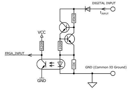
Internal Schematic
Following scheme is internal scheme of Digital Input signal flow inside the camera.
Timing
Typical measured input delay between Digital Input to FPGA Input
| Edge Type | V INPUT [V] | Typ. delay [μs] |
| Rising | 5 | 1.6 |
| Rising | 10 | 1.7 |
| Falling | 5 | 7.8 |
| Falling | 10 | 10.7 |
| Falling | 24 | 12.7 |
NOTE: Measured at: Ambient Temperature 25°C
24V GPI
Supported cameras
| Camera model | HW Revision |
| MQ003xG-CM | <4 |
| MQ013xG-E2 | <6 |
| MQ013xG-ON | <3 |
| MQ022xG-CM | <6 |
| MQ042xG-CM | <6 |
Input Levels
Input levels according IEC 61131-2, Type 1
| State | V-in-min [V] | V-in-max [V] | I-max [mA] |
| Off (0) | -3 | 5 | 0.004 |
| Transient | 5 | 15 | 4 |
| On (1) | 15 | 30 | 12 |
- Input level Vin represents amplitude of the input signal.
- Voltage levels referenced to common ground pole GND (see Pinning).
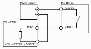
Wiring
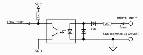
Internal Schematic
Following scheme is internal scheme of Digital Input signal flow inside the camera.
Timing
Typical measured input delay between Digital Input to FPGA Input
| Edge Type | V INPUT [V] | Typ. delay [μs] |
| Rising | 15 | 1.4 |
| Rising | 20 | 0.6 |
| Falling | 15 | 5.3 |
| Falling | 20 | 7.8 |
NOTE: Measured at: Ambient Temperature 25°C