Output levels definition
| State | Open Collector Switch State | R [Ohm] | Conditions |
| On (1) | ON - Transistor is conducting | max 160 | for I output > 5mA |
| Off (0) | OFF - Transistor is not conducting | min 100k |
| Maximum sink current [mA] |
| 25 |
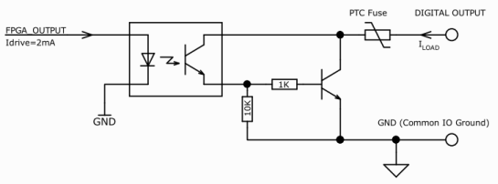
Digital output has an open collector switching transistor with common IO Ground.
See Digital Output Wiring for more details.
Following scheme is internal scheme of Digital Output signal flow inside the camera.
When Output is in On state - typical transfer characteristic of output is as on following figure:![]()
Typical input delay between FPGA_Output to Digital Output
| Ioutput [mA] | Typ Delay Off->On [μs] | Typ Delay On->Off [μs] | Note |
| 2 | 0.55 | 184 | TAMBIENT=25°C |
| 5 | 0.55 | 182 | TAMBIENT=25°C |
| 10 | 0.55 | 133 | TAMBIENT=25°C |
| 25 | 0.55 | 113 | TAMBIENT=25°C |